Microprocessors are defined as a computer’s central processing unit, usually contained on a single integrated circuit (Wyant and Hammerstrom, 193). In plain English this simply means that a microprocessor is the brain of a computer and it is only on one chip. Winn L. Rosch compares them to being an electronic equivalent of a knee-joint that when struck with the proper digital stimulus will react in the exact same way each time (Rosch,37). More practically a microprocessor is multitudinous transistors squeezed onto as small a piece of silicon as possible to do math problems as fast as possible.
Microprocessors are made of many smaller components which all work together to make the chip work. A really good analogy for the way the  inner workings of a chip operate can be found in How Microprocessors Work. In their book, Wyant and Hammerstrom describe a microprocessor as a factory and all of the inner workings of the chip as the various parts of a factory (Wyant and Hammerstrom, 71-103). Basically a microprocessor can be seen as a factory because like a factory it is sent something and is told what to do with it. The microprocessor factory processes information. This most basic unit of this information is the bit. A bit is simply on or off. It is either a one or a zero. Bits are put into 8 bit groups called bytes. The number 8 is used because it is offers enough combinations to encode our entire language (2^8=256). If only 4 bits are used only (2^4=16) combinations would be possible. This is enough to encode 9 digits and some operations. (The first microprocessors powered calculators) A half byte is called a nibble and consists of 4 bits. In the world of computer graphics the combination of bits is easier seen. In computer graphics bits are used to make color combinations, thus with more bits more colors are possible. Eight bit graphics will display 256 colors, 16 bit will display 65,536, and 24 bit graphics will display 16.7 million colors. The bus unit is described as the shipping dock because it controls data transfers, and functions between the individual pieces of the chip. The part of the chip that performs the role of a purchasing department is called the prefetch unit. It’s job is to make certain that enough data is on hand to keep the chip busy. The decode unit performs the role of a receiving department.
It breaks done complicated instructions from the rest of the computer into smaller pieces that the chip can manipulate more readily. The control unit is compared to the person who oversees the workings of the entire factory. It is the part of the chip that keeps all the other parts working together and coordinates their actions. The arithmetic logic unit is compared to the assembly line of the factory. It is the part of the microprocessor that performs the math operations. It consists of circuitry that performs the math and the registers which hold the necessary information. The memory management unit is likened to the shipping department of this digital factory. It is responsible for sending data to the bus unit. Together all of the individual pieces support each other to make this digital symbiosis work as fast as possible.
To an outsider, computer nerd vernacular and all other forms of computer people esoteric may or may not be considered frightening. Probably the most confused term in microprocessor performance is Megahertz (MHz). Basically these are millions of cycles per second. This is a measurement of chip speed but is better considered the RPM of the chip (Knorr, 135). For example a 486 100 MHz processor cannot touch the speed of a Pentium running at only 60 MHz. This is because the Pentium packs more power and can do more per clock cycle. The computer bus is the data line that connects the microprocessor the rest of the computer. The width of the bus (how many bits it consists of) controls how much data can be sent to the chip per clock cycle. MIPS or millions of instructions per second is simply how many instructions the chip can perform in one second divided by 1,000,000. RISC is a commonly used term in the computing world also. It is an acronym for Reduced Instruction Set Computer. Chips that incorporate RISC technology basically rely on simplicity to enhance performance. Motorola chips use this technology. The opposite of RISC is CISC which stands for Complex Instruction Set Computer. These chips use more hardwired instructions to speed up the processing process. All Intel PC products fall into this category. Pipelining, superscalar architecture, and branch prediction logic are currently technological buzzwords in the computer community presently. These technologies can be found in newer chips. Pipelining allows the chip to seek out new data while the old data is still being worked on (Wyant and Hammerstrom, 161). Superscalar architecture allows complex instructions to be broken down into smaller ones and then processed simultaneously through separate pipelines (Wyant and Hammerstrom, 161-163). Branch prediction logic uses information about the way a program has behaved in the past to try to predict what the program will do next (Wyant and Hammerstrom, 165). Bus speed is simply the speed in MHz at which the data bus travels. This is relative to how fast the microprocessor can communicate with the rest of the computer. A register is the part of the chip that hold the information that the chip is currently manipulating. The width of the register in bits is relative to how much data the chip can process simultaneously. Using very long instruction words is simply using instructions larger than 16 bits to increase the amount of data the chip can be sent at once. A new tool being used in making chips run faster is to place a cache on the chip. This cache is for holding data that the chip is most likely to need first. Since the data is stored inside the chip the access time is lowered dramatically. In the future more and more of the computer will be integrated on the main processing unit. Line width is also a sign of the technological times. It is simply how small the smallest feature is on a chip. Basically the smaller the lines the more transistors can be squeezed onto the wafer and thus increase performance while cutting manufacturing costs.
Non-technological issues also have a major effect on the microprocessing world. One such issue is heat. This may sound trivial but a Pentium  chip can and will burn the skin of a person who touches one that has been running for longer than a few minutes. Without a fan most modern chips will melt and or destroy themselves. To combat this, large aluminum heat sinks are attached to the chips and a large fan is placed in the case. Some users prefer to use a separate fan above the heat sink for added insurance. Operating voltages can also add to the heat problem. Chips run from either 3.3 or 5 volts. Three and three tenths volts is preferred now because with less power less heat is generated and in the case of laptops battery life is extended.
Credit for the invention of the microprocessor is given to Intel. This first microprocessor was the 4004 and was released in 1971. This single chip matched the performance of the room size computer ENIAC from the fifties (Wyant and Hammerstrom, 19). This chip could only support a four bit bus. These four bits only offered the possibility of coding 16 symbols (2^4=16). Sixteen symbols was enough for digits 1-9 and then some operators. This limited the 4004 to calculator usage. The 4004 ran at 108 kHz which is 1/10 of 1 MHz (Rosch, 66). The smallest feature on the chip measured 10 microns and contained 2300 transistors.
The next generation of Intel chips used a 8 bit data bus. The first member of this generation was released in 1972 and was called the 8008. This chip was the same as the 4004, but it had 4 more bits on each register. This chip had enough bits to code 256 symbols (2^8=256). This number is easily enough to encode our alphabet, numerals, punctuation marks, etc. The 8008 also ran a little faster than the 4004 with its speedy clock of 200 kHz. The 8008 contained 3500 transistors and had line widths 10 microns. Both chips had a MIPS of 0.06 (Rosch, 66).
The next member of the Intel family was born in 1974 and was called the 8080. This chipped was intended to handle byte sized data (8 bit). The 8080 contained 6000 transistors and had 6 micron technology. This chip performed at 0.65 MIPS and had an internal clock speed of 2 MHz. This was one of the first chips to have the capabilities of running a small computer (Rosch, 66).
In June of 1978 the 8086 family was released by Intel. These chips used 16 bit registers. The fastest chip in this series ran at 10 MHz and could execute.75 MIPS. This chip forced engineers of the time to begin developing fully 16 bit devices, which were more expensive than their 8-bit brethren. Because of this, the 8086 family was considered ahead of it’s time (Rosch, 67-68).
A year later Intel introduced the 8080. This chip was a step backwards in chip evolution with it’s 8 bit data bus. The 8080 could process.64 MIPS with it’s 6000 transistors. The 8080 used 6 micron technology. This chip is worth mentioning primarily because IBM chose to use it in it’s first personal computer. IBM was able to use the 8088 with existing 8 bit hardware, which was more cost effective. Later IBM began using the 8086 in it’s newer systems (Rosch, 68).
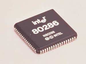
In 1982 Intel released the 80286. The 286 family was available in clock speeds of 8, 10, and 12 MHz that could execute 1.2, 1.5, and 1.66 MIPS respectively. The 80286 contained 134,000 transistors with 1.5 micron technology. These chips all used a 16 bit data bus and were used by IBM in it’s AT models. This was also the first chip to use virtual memory, or using disk space as RAM (Random Access Memory). To allow full downward compatibility the 286 was designed to have two operating modes. These modes are real and protected mode. Real mode mimics the operation of an 8086. Protected mode allows multiple applications to be run simultaneously and not interfere with each other (Rosch, 70-71).
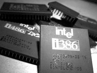
The next member to the Intel family was added in November 1985 and was the 80386. These chips are offered in speeds of 16, 20, 25, 33 MHz and can process 5.5, 6.5, 8.5, and 11.4 MIPS respectively. The number of transistors in the 80386 is 275,000 with 1.5 micron technology. The 386 family doubled the register size to 32 bits. Also the 386 uses 16 bytes of prefetch cache that the chip uses to store the next few instructions. The 386 has three models which are called the 386DX, 386SX, and the 386SL. The 386DX was the original and most powerful. The 386SX is a more economical sibling to the DX. It is basically scaled down, less powerful DX. Also the SX uses a 16 bit data bus. The SL also uses 16 bit buses but it includes power saving features targeted at notebook usage. The SL uses 1.0 micron technology and contains 855,000 transistors (Rosch, 72-78).
The 80486 family was introduced in April 1989 and became a “better 386” (Rosch, 78). The 486 was originally released in a DX model with speeds of 25, 33, and 50 MHz that processed 20, 27, and 41 MIPS respectively. The DX also contains a math coprocessor or floating point unit that helps speed up math operations. The 486DX uses a 32 bit bus and contains 1,200,000 transistors. It uses 1.0 micron technology in the 25 and 33 MHz models, but in the 50 MHz model uses 0.8. The next to be released was the 486SX. The SX was designed to cut cost at the price of not having a math coprocessor. As a result the SX will not perform as well as the DX in math intensive operations. The SX contains 1,185,000 transistors and uses the same technology as the DX. The SX is available in 16, 20, 25, and 33 MHz models that process 13, 16.5, 20, and 27 MIPS respectively. To add the power of a FPU (Floating Point Unit) to the SX Intel released the OverDrive upgrade processors in March 1992. The first, the 486DX2, incorporated clock doubling technology. These chips operate at double the bus speed. These chips are available in 50 and 66 MHz models that can process 41 and 54 MIPS respectively. The 50 MHz model was designed to replace the 25 MHz 486SX and the 66 MHz model was for the 33 MHz 486SX. The OverDrive chips contain 1.2 million transistors. The next to be released was the SL model which was, like the 386SL, targeted at laptop usage. The SL contains 1.4 million transistors and can process 15.4, 19, and 25 MIPS while running at 20, 25, and 33 MHz respectively. The 486DX4 was the next OverDrive chip to be released. It contains clock tripling technology. The DX4 can turn a 33 and 25 MHz 486’s into DX4-100 and DX4-75 respectively. These chips can process 60 and 81 MIPS running at 75 and 100 MHz respectively. The DX4 uses 0.6 micron technology (Rosch 84-85).
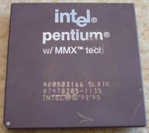
The next addition to the Intel family was the Pentium. The Pentium was originally released in a 60 MHz model that operated at 5 volts. This  chip contains 3,100,000 transistors and can process 100 MIPS. The next to be released was the 66 MHz model. It uses the same technology but is a 3.3 volt chip and can process 112 MIPS. Currently the Pentium is available in 66, 75, 90, 100, 120, 133, 150, and 166 MHz models. Beyond the 75 all Pentiums use 0.6 micron technology. A 180 MHz is slated for future release. The Pentium family is, like all of Intel’s chips, uses CISC technology. Also they use pipelining, superscalar architecture, and branch prediction logic. A Pentium OverDrive is also available for upgrading 486 systems to Pentium technology. The Pentium OverDrive is available in a 63 and 83 MHz version (Rosch, 85-87).
After the Pentium, the only more advanced chip Intel has for personal use is the Pentium Pro. This chip has only been available for a short time and is targeted at workstation and server usage. It will only run Windows NT and native 32 bit software at an increased speed. When using 16 bit software, the less powerful Pentium will outperform its larger sibling. The Pentium Pro also contains 256K (256,000 bytes) of on chip cache memory.
The only certainty in the future of microprocessors is constant improvement. One prediction for the future is called Moore’s Law. This prediction is named after Intel cofounder Gordon Moore who presented it in 1965. The law states the transistor densities will double every two years. Line width is also continuing to shrink and is estimated to be at 0.2 microns by the turn of the century. When all is considered the future of computers is very exciting (Wyant and Hammerstrom, 184-185).
Bibliography
Knorr, Eric. “From 586 to Pentium Pro: Choosing Your Dream PC.” PC World February 1996: 133-142.
Rosch, Winn L. The Hardware Bible. Indianapolis: SAMS, 1994.
Wyant, Gregg, Hammerstrom, Tucker. Intel, How Microprocessors Work. Emeryville: Ziff-Davis, 1994.
